


During production, printed circuit boards (PCBs) are visually inspected by automated optical inspection (AOI) systems, which employ a camera to scan the board in incredibly fine detail to look for any flaws or failures. In order to replace the human eye, AOI integrates optics, mechanics, electronic control, and software. PCBs are becoming smaller and more intricate in the real world; even a relatively basic board can include thousands of soldered parts. In today’s cutthroat PCB production climate, AOI keeps an eye on the quality of PCB manufacture and makes necessary corrections in the process flow.
A machine-based method called automated optical inspection (AOI) is used to test and examine PCBs for potential flaws such surface, dimensional, and component positioning issues. It goes without saying that AOI plays a crucial role in inspecting the printed circuit board after assembly as it is difficult and impossible to physically inspect the increasingly complex circuit boards. Additionally, it has a significant impact on achieving the required product quality on the production line at a reasonable cost.
AOI systems are available in a variety of forms, each appropriate for a particular type of inspection task. The kind of imaging technology these systems employ is a crucial differentiator. AOI systems can be classified as either 2D or 3D systems. Each has distinct advantages, and the decision between them frequently depends on the particulars of the current inspection work.
2D AOI Systems
The most popular kind of AOI now in use is two-dimensional AOI systems. These devices take pictures of the item being examined using 2D cameras. This kind of AOI is especially good at finding a variety of surface-level flaws, including soldering faults, misaligned components, missing components, and erroneous components.
To conduct inspections, the 2D AOI system mostly makes use of traditional image and pattern recognition technology. The procedure normally entails taking a picture of the examined item, which is commonly a printed circuit board (PCB), and comparing it to the data that has been stored for a perfect, defect-free PCB. The system can identify any inconsistencies or flaws on the actual PCB thanks to this comparison.
3D AOI Systems
A more sophisticated development in AOI technology is represented by three-dimensional AOI systems. These systems create a thorough topographical map of the inspected object using 3D imaging technology, which is usually based on either laser triangulation or structured light projection.
Laser triangulation is the process of projecting a laser line onto an object’s surface, then taking a picture of the line with a camera. The technology can determine the surface’s height profile by examining the line’s distortion. This technique can measure heights with a resolution of up to 1 micron, making it incredibly accurate. However, because the laser line must be scanned across the whole surface of the object, it is somewhat slow.
A quicker option to laser triangulation is structured light projection. With this technique, a light pattern is projected onto the object’s surface, and a camera is used to take a picture of the warped pattern. The system can determine the surface’s height profile by examining the distortion in the pattern. With a typical height resolution of about 10 microns, this technique is slightly less accurate but faster than laser triangulation.
Automated Optical Inspection (AOI) systems are designed to quickly identify common PCB assembly defects during SMT production. Typical issues AOI can detect include:
Positional precision: As component sizes shrink, manufacturing and inspection equipment positional accuracy becomes more crucial. Additionally, as a general rule, AOI systems should have sub-pixel precision, which ensures that there is sufficient accuracy for the system to identify the slight positional variations that may cause a 01005 defect.
Low cost: By increasing the PCB pass rate, AOI testing helps lower PCB costs.
Programmable lighting: In any machine vision application, lighting must produce the intended effects. It is impossible to locate a single light source that can identify every problem state given the dynamic nature of electronics manufacturing. In order to ensure that the component and PCB layouts have the broadest defect coverage, a dynamic light is crucial. The AOI test may set up highly customisable light arrays within the inspection software, which reduces the cost of light-emitting diodes. Additionally, the AOI test may dynamically expand the image’s contract, making it simple to detect a wide range of defect circumstances with various colours at various angles. Lighting programming is a crucial tool for ensuring the broadest detection range.
Multiple inspection objects: The AOI test is effective for PCB assembly as well as PCBs. Regarding PCBs, it inspects for flaws such shorts, openings, and inadequate solder. But when it comes to PCB assembly, it looks at things like values, polarity, and component soldering.
Network-capable software: Data collection and retrieval are key components of any AOI system. The data may be stored in a database, an image collection, a written output, or a mix of many formats. Most AOI systems have a basic purpose of gathering data, but retrieving the information is frequently more complicated and depends on how the manufacturing line is set up.
Solder Joints Not Visible: Many “gremlins” in electronics originate from them. AOI machines frequently miss circuit faults. Solder joints may not be visible.
Misjudgment: Defect detection is slow for the majority of AOI devices. The AOI devices that employ scanning techniques are quick to find flaws.
Misjudgment is more likely, though. It may be caused by solder junctions encircled by elements, sections covered by other components, or distinct light colors. AOI can only identify locations that are directly illuminated by light.
Fixtures Are Expensive and Hard to Update: The majority of AOI software is unable to solve complex issues. As a result, they won’t be able to offer fixes. When it comes to updating AOI systems, obtaining an updated version becomes difficult. The AOI system is exceedingly costly and difficult to upgrade or run.
Test Access Gets Harder: Only flaws with challenging failure mechanisms, including glue or seal flaws, are detected by AOI. It is necessary to program defect detection capabilities since they are rigid.
AOI is crucial to quality assurance and control. It saves time and resources in addition to producing accurate and quick results. Most importantly, the outcomes are automatically recorded and repeatable. AOI systems can be accurately adjusted to the parameters of quality control inspections and learn extremely quickly. The user can examine the defective workpiece by hand if the machine detects a flaw. If the fault was accurately identified, it is a real defect, and the AOI system saves this information. It is a pseudo fault, nevertheless, if the user determines that the part’s flaw is still within tolerances. Additionally, the machine learns from this and will no longer recognise this flaw as an issue going forward.
Reliable embedded boards manufactured with SMT production, AOI inspection, and industrial-grade quality standards.
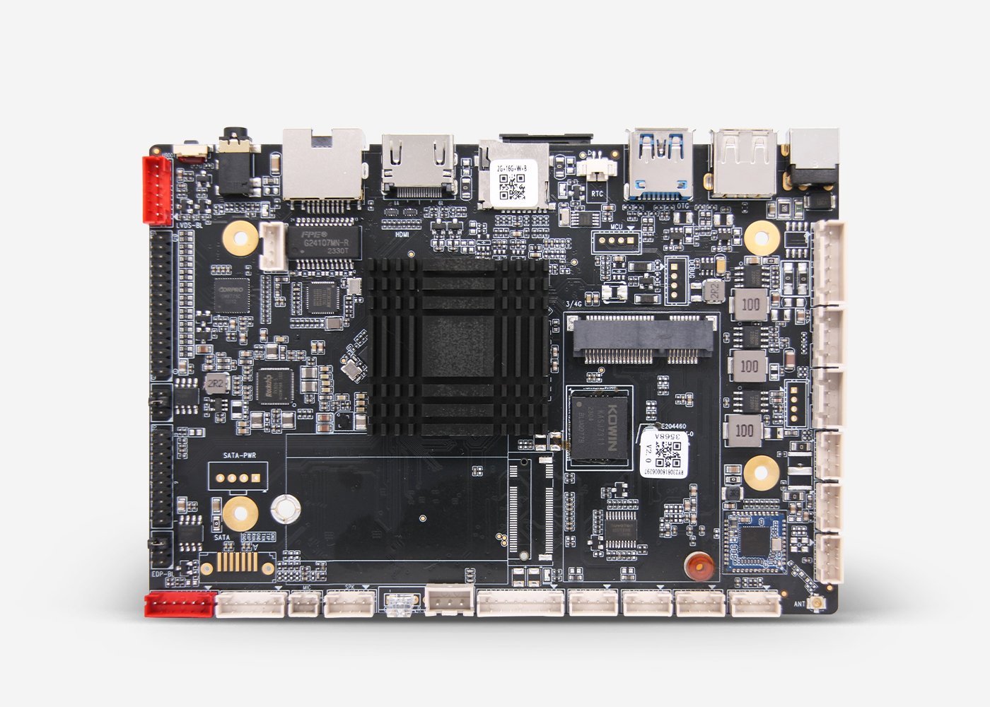
Stable ARM motherboard for kiosks, HMI systems, automation terminals, and smart devices.
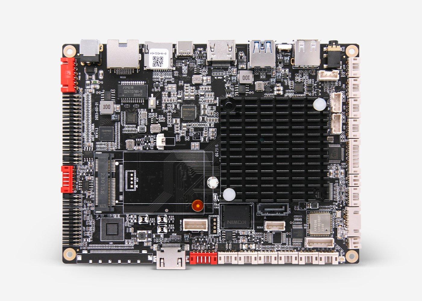
High-performance motherboard for machine vision, AI terminals, and edge computing systems.
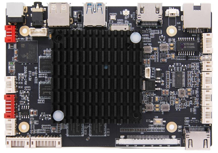
Commercial motherboard for smart displays, digital signage, and interactive touch terminals.

We go into great detail about inspection technologies on our resources page, but to put it simply, the procedure entails taking high-resolution photos of products, which are then meticulously compared to a reference. For an inspection system to be effective, a number of processes must be flawlessly coordinated. Advanced features like high-accuracy inspection and measurement are provided by automated optical inspection systems, which must be installed by experts because even a tiny mistake can result in expensive issues.
Algorithms for classifying and detecting defects
Algorithms for defect identification and categorisation are essential to automated optical inspection systems. Finding flaws in the manufacturing process requires optical examination. These algorithms use the collected images to precisely classify and identify flaws. To provide quality control, AOI systems must be integrated into the production line.
Techniques for image processing and acquisition
AOI systems can take high-resolution pictures of the product being inspected using one or more cameras placed at various angles. After that, these photos are examined by specialized software that use complex algorithms to find any irregularities or departures from the expected standards. The program can distinguish between genuine flaws and acceptable variants, highlighting possible flaws for more investigation or remedial action. To increase the precision and effectiveness of AOI systems, sophisticated image processing methods including 3D imaging and machine learning are now being employed.
Automated optical inspection is used for quality assurance in these application areas, among others:
In conclusion, it is capable of inspecting the quality of the boards that are produced at any PCB fabrication facility. This is the only way they can keep an eye on quality and make necessary corrections to the process in order to prevent it from affecting other boards. In this sense, X-ray and automatic optical inspection are essential tools for the PCB manufacturing sector.
Custom motherboards, panel PCs, AI edge devices, kiosks and display hardware with reliable manufacturing and global delivery.
Automated optical inspection, or AOI, is utilised in the modern industrial sector to improve inspection accuracy and uniformity while cutting production time and costs. It is very helpful in upholding quality standards, particularly in high-speed production lines where manual inspection is not feasible.
AOI systems can match the speed of high-speed manufacturing lines by inspecting hundreds to thousands of components every minute. Additionally, they offer real-time feedback, making it possible to make changes right away if flaws are found. This enhances the quality of the final product and lowers waste.
AOI is a visual inspection technology widely used in the electronic manufacturing industry to enhance product quality by efficiently identifying defects.
A stop-and-go method is used to move one or more cameras over the area to be inspected while pointing at the part. Inline and atline systems can both use AOI with cameras or scanners. When components or assemblies are measured and quality-controlled on the shop floor, this is referred to as inline.
Automated Optical Inspection (AOI) is a crucial technology used in modern manufacturing to ensure products are free from defects. AOI systems utilize advanced cameras, lighting, and image processing algorithms to analyze components with incredible accuracy.


